by Walter Crismareanu
Breakthrough in semiconductors. Graphene had no bandgap, until now!
“We now have an extremely robust graphene semiconductor with 10 times the mobility of silicon, and which also has unique properties not available in silicon.”
—Walter de Heer
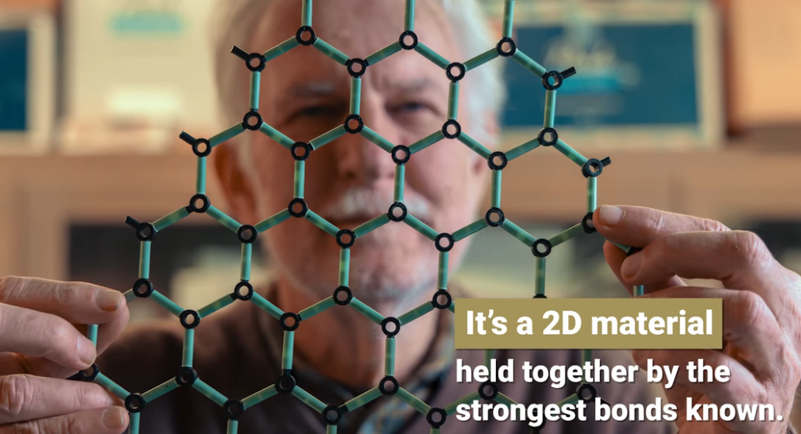
Researchers have created the first functional semiconductor made from graphene, a single sheet of carbon atoms held together by the strongest bonds known.
The breakthrough throws open the door to a new way of doing electronics.
Who did it?
“Walter de Heer, Regents’ Professor of physics at Georgia Tech, led a team of researchers based in Atlanta, Georgia, and Tianjin, China, to produce a graphene semiconductor that is compatible with conventional microelectronics processing methods—a necessity for any viable alternative to silicon.”
They persisted in perfecting the material at Georgia Tech and later in collaboration with colleagues at the Tianjin International Center for Nanoparticles and Nanosystems at Tianjin University in China. De Heer founded the center in 2014 with Lei Ma, the center’s director and a co-author of the paper.”
Graphene
“In its natural form, graphene is neither a semiconductor nor a metal, but a semimetal. A band gap is a material that can be turned on and off when an electric field is applied to it, which is how all transistors and silicon electronics work. The major question in graphene electronics research was how to switch it on and off so it can work like silicon.
But to make a functional transistor, a semiconducting material must be greatly manipulated, which can damage its properties. To prove that their platform could function as a viable semiconductor, the team needed to measure its electronic properties without damaging it.”
How they did it?
“They put atoms on the graphene that “donate” electrons to the system—a technique called doping, used to see whether the material was a good conductor. It worked without damaging the material or its properties.
The team’s measurements showed that their graphene semiconductor has 10 times greater mobility than silicon. In other words, the electrons move with very low resistance, which, in electronics, translates to faster computing. “It’s like driving on a gravel road versus driving on a freeway,” de Heer said. “It’s more efficient, it doesn’t heat up as much, and it allows for higher speeds so that the electrons can move faster.””—
Result
“A long-standing problem in graphene electronics is that graphene didn’t have the right band gap and couldn’t switch on and off at the correct ratio,” said Ma.
Our technology achieves the band gap, and is a crucial step in realizing graphene-based electronics.””
Epilogue
“You’re actually using the properties of electrons that are not accessible in silicon, so this is really a paradigm shift, it’s a different way of doing electronics.”Walter de Heer
MY2CENTS (Walter)
- This is a huge breakthrough, as a collaboration project between USA & China!
- It would be nice to hope, the commercialization of this technology could come earlier than expected.
more Thinking Along with Walter

My 2 Cents: Human Evolution & AI: A Symbiosis in the Long Run?
Is AI the next step in human evolution? If so, then you too can become a robot and live forever
Graphene materials for fabrication of robots: by Science Direct
“The robot’s fabrication is a complex process involving the preparation of many components and then their assembly. If all the components are made from graphene derivatives, then their liaison is very successful and useful.
“Among many parts, skin is a very important part of soft robots and electronic skin is the best choice for this purpose. The purpose of skin is to collect outside information about its surroundings, through tactile sensors and high-performance tactile sensors.”
Researchers at the Georgia Institute of Technology
by Science Daily
have created the world’s first functional semiconductor made from graphene, a single sheet of carbon atoms held together by the strongest bonds known. Semiconductors, which are materials that conduct electricity under specific conditions, are foundational components of electronic devices. The team’s breakthrough throws open the door to a new way of doing electronics.
Their discovery comes at a time when silicon, the material from which nearly all modern electronics are made, is reaching its limit in the face of increasingly faster computing and smaller electronic devices. Walter de Heer, Regents’ Professor of physics at Georgia Tech, led a team of researchers based in Atlanta, Georgia, and Tianjin, China, to produce a graphene semiconductor that is compatible with conventional microelectronics processing methods — a necessity for any viable alternative to silicon.
GRAPHENE
In its natural form, graphene is neither a semiconductor nor a metal, but a semimetal. A band gap is a material that can be turned on and off when an electric field is applied to it, which is how all transistors and silicon electronics work. The major question in graphene electronics research was how to switch it on and off so it can work like silicon.
But to make a functional transistor, a semiconducting material must be greatly manipulated, which can damage its properties. To prove that their platform could function as a viable semiconductor, the team needed to measure its electronic properties without damaging it.
They put atoms on the graphene that “donate” electrons to the system — a technique called doping, used to see whether the material was a good conductor. It worked without damaging the material or its properties.
The team’s measurements showed that their graphene semiconductor has 10 times greater mobility than silicon. In other words, the electrons move with very low resistance, which, in electronics, translates to faster computing. “It’s like driving on a gravel road versus driving on a freeway,” de Heer said. “It’s more efficient, it doesn’t heat up as much, and it allows for higher speeds so that the electrons can move faster.”
The team’s product is currently the only two-dimensional semiconductor that has all the necessary properties to be used in nanoelectronics, and its electrical properties are far superior to any other 2D semiconductors currently in development.
“A long-standing problem in graphene electronics is that graphene didn’t have the right band gap and couldn’t switch on and off at the correct ratio,” said Ma. “Over the years, many have tried to address this with a variety of methods. Our technology achieves the band gap, and is a crucial step in realizing graphene-based electronics.”